Photonic Switch Model for Data Applications
Project Description
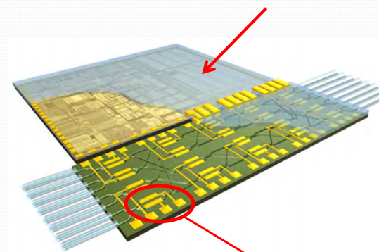
Switching fabrics in data centers that rely on traditional electrical switches face scaling issues in terms of power consumption. Fast optical switches based on a silicon photonics platform can enable the high port speed and high interconnection density needed while still maintaining a small footprint and low power consumption.
The interconnect fabric is taking an ever-more dominant portion of the power budget. Optical interconnects are already used today within data centers for rack to rack interconnection to overcome the limits of electrical signaling. However, the switches interconnecting these racks have inadequate capacity to continue to scale with complementary-metal-oxide semiconductor (CMOS)-based technology due to fundamental limitation of on-chip interconnects, power consumption and pin count of scheduler application-specific integrated circuits. Further, not only does the switch fabric require significant power, but the conversion from the optical signal to electrical and back again (OEO) adds a significant amount of power and space. We present here a unique switching technology that allows for high radix and high bandwidth, which is not achievable in conventional electrical interconnects, while dissipating very low power. We achieve these diametrically opposing goals by utilizing the large-bandwidth enabled by optics fabricated in a cost-efficient CMOS platform. Furthermore, we integrate conventional CMOS electronics within the optical platform using a chips last integration process.
The students will be involved in the following tasks
- Literature reading and search on existing switching technologies
- Build a switch model, a transmitter and receiver in teams of two using circuit simulator TI- TINA
- Each team will prototype the switch circuit, transmitter and receiver circuit using breadboard and discrete circuit elements.
- Measure the functionality